Home
si gaas, 7. Consider two semiconductors, Si GaAs. | Chegg.com, GaAs – – doped – 1” Dia.
-
 Si GaAs In each case, identify the valence and bands and identify the band gap in the two") SOLVED: electronic band structure for Si and GaAs is shown below: i) Si GaAs In each case, identify the valence and bands and identify the band gap in the two
SOLVED: electronic band structure for Si and GaAs is shown below: i) Si GaAs In each case, identify the valence and bands and identify the band gap in the two
-
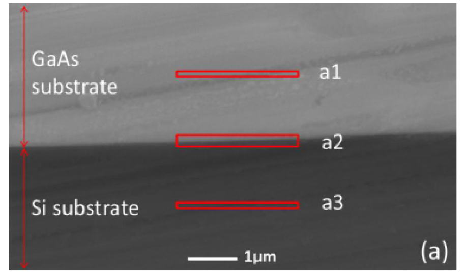
 density GaAs/Si rectifying heterojunction by defect free Epitaxial Lateral on Tunnel Oxide from nano-seed | Scientific Reports
-
 FCMN: Mobility & Activation depth for Si:GaAs at – Active Layer Parametrics, Inc.
-
 SI-GaAs physical constants used in | Table
-
 Solved effective density of Ge, Si, and GaAs | Chegg.com
-
 GaAs - - lifetime, single crystal orientation, PID, automation and more
-
 - AnySilicon") Gallium Arsenide (GaAs) - AnySilicon
Gallium Arsenide (GaAs) - AnySilicon
-
 1 Properties of Si, SiC, and GaN | Download Scientific Diagram
-
: Inder Bahl, I J Bahl: 9781608077113: Amazon.com: Books") Control Using Si, GaAs, and GaN Technolgoies (Artech House Mcrowave Library): Inder Bahl, I J Bahl: 9781608077113: Amazon.com: Books
Control Using Si, GaAs, and GaN Technolgoies (Artech House Mcrowave Library): Inder Bahl, I J Bahl: 9781608077113: Amazon.com: Books
-
 Be, Te, and Si Doping of GaAs Nanowires: Theory Experiment | The of Physical Chemistry
-
 Comparison between and GaAs photocurrents normalized to a.u. ͒ . | Download Scientific Diagram
-
 Physical properties Si, GaAs, SiC, GaN, diamond. | Download Scientific Diagram
-
 thin film resistance sensors on GaAs Semantic Scholar") Figure 3 from Si/Ni(Pt) thin film resistance sensors on GaAs Semantic Scholar
Figure 3 from Si/Ni(Pt) thin film resistance sensors on GaAs Semantic Scholar
-
 Physical properties Si, GaAs, SiC, GaN, diamond. | Download Scientific Diagram
-
-
: Inder Bahl, I J Bahl: 9781608077113: Amazon.com: Books") Control Using Si, GaAs, and GaN Technolgoies (Artech House Mcrowave Library): Inder Bahl, I J Bahl: 9781608077113: Amazon.com: Books
Control Using Si, GaAs, and GaN Technolgoies (Artech House Mcrowave Library): Inder Bahl, I J Bahl: 9781608077113: Amazon.com: Books
-
 bandgap operation of a GaAs/Si photoelectrode - ScienceDirect
-
 Applied Sciences | | Multi-Energy Valley Scattering Characteristics for a SI-GaAs-Based Terahertz Photoconductive Antenna in Linear Mode
-
 Inorganics | | Improved Tunneling Property of p+Si Nanomembrane/n+GaAs Heterostructures through Ultraviolet/Ozone Treatment
-
 Gallium -
-
 GaAs – – doped – 1” Dia.
-
 List of various properties of Si, GaAs, and GaN channel materials... | Download Table
-
![6: Energy structures of GaAs and as in [5]. A... | Download Scientific Diagram](https://www.researchgate.net/publication/276198395/figure/fig4/AS:669451464740888@1536621075947/Energy-band-structures-of-GaAs-and-silicon-as-in-5-A-semiconductors-absorption.png "6: Energy structures of GaAs and as in [5]. A... | Download Scientific Diagram") 6: Energy structures of GaAs and as in [5]. A... | Download Scientific Diagram
6: Energy structures of GaAs and as in [5]. A... | Download Scientific Diagram
-
 A pulse compression diode based on SI-GaAs material
-
 - YouTube") Materials Si, GaAs) - YouTube
Materials Si, GaAs) - YouTube
-
 GaAs solar cell on Si substrate with good ohmic GaAs/Si interface direct wafer bonding - ScienceDirect
-
 7. Consider two semiconductors, Si GaAs. | Chegg.com
-
 Comparing Ge and caleulate the intrinsic | Chegg.com") Solved 1) Comparing Ge and caleulate the intrinsic | Chegg.com
Solved 1) Comparing Ge and caleulate the intrinsic | Chegg.com
-
 1. Absorption lengths for c-Si and GaAs. Note that the bandgap... Download Scientific Diagram